If you adhere to proper nutrition, then avocados are probably in ...


As you know, the world of electronics has conquered many people. And as many experts say, "Electronics is the future." Every year, thousands of different boards roll off the assembly lines of factories. Many people are fond of soldering boards, repairing, some people even design some kind of electronic devices at home. But few people know that the board itself can be made at home. This requires a few things and patience.
And what things are needed to make a board at home, how to make a board in general will be described in this article.
Let's start with what you need to make a printed circuit board: Photoresist, transparent film from Lamond, heated ultraviolet, board template, spray, for toner booster, caustic soda, for washing off an unexposed photoresistor, cotton pads, alcohol and acetone, as well as laminate, for gluing a photoresistor. As the case progresses, everything about everything will be told what and why is needed. The first thing to say is that the photoresist is the basis of the board. And the spray is needed for the board pattern amplifier. It is also worth noting that a special program is required to make a drawing of the printed circuit board itself. In my case, I use the Sprint Layout 6 program. On this program, we draw a drawing of the board, that is, the board itself. Also on the same program it is necessary to make a solder mask, that is, places where electronic elements (transistors, microcircuits, etc.) will be soldered.
Further, when the board is printed on a film, that is, a bar is inserted instead of paper, it must be treated with toner. The drawing will be clearer and more understandable. Before processing the drawing, it must be well dried. After the drawing has dried, it must be sprinkled with toner (In my case, I use Kdensit toner) and left to dry for 10-15 minutes. After 15 minutes of drying, the drawing will be perfectly black. I also want to say that it’s straight, you don’t need to fill the drawing with toner. It must be processed as needed. In the same way, it is necessary to process the solder mask. If it happens that the toner is faded in some places, then it can be tinted with an ordinary felt-tip pen. Sometimes there are fading, when the printer prints poorly.
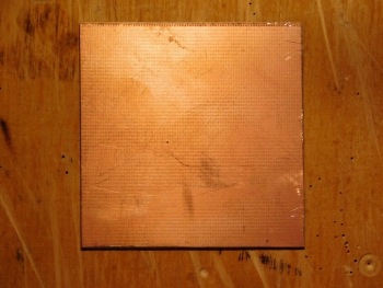
Next, take the photoresist. It is advisable to keep it permanently in the refrigerator, in a dark film. We take our photoresistor, and cut it according to the dimensions of our board. If desired, you can cut off a little more (along the edges with a margin).
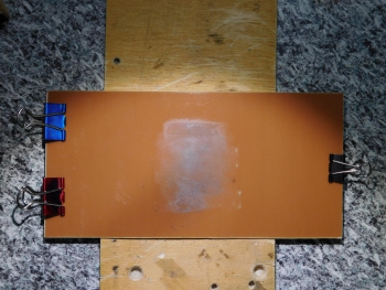
Next, you need to stick the photoresistor on the board. This must be done under cold water. Under water, this must be done so that there are no wrinkles. The photoresistor itself is a film glued on top of each other, like a sticker that is often found in chewing gum. So, on one corner of the photoresistor we stick ordinary paper tape and peel it off the base. But we do not glue all. Next, we lower the board under water, and remove the protective film of the photoresistor, and at the same time stick it on the board. We glue thoroughly so that there are no air bubbles under it. During the sticker process, it can be peeled off and re-glued as you like. The main thing is to do it under cold water, and so that there are no folds and air bubbles. Also, the boards must be perfectly washed so that there are no specks, no streaks, and nothing at all. Boards can also be washed with soap and water, but without any household chemicals. After gluing under water, it is necessary to smooth out all the folds. This can be done with an ordinary construction, but plastic spatula. Excess pieces of the photoresistor at the edges must be cut off. In the process of leveling and wiping water, we turn on and warm up the elaminer so that it warms up. You need to heat it up to 125 degrees.
Next, we take our board pattern and put it with the printed side on the elaminator, that is, the glossy side down and the pattern out. Next, take the board and place it on the drawing with the side of the photoresistor. It is necessary to put, so to speak, exactly the same, so in the process we level the board so that it lies evenly on the drawing. Next, carefully press the board to the drawing. If someone cannot, then you can put a brick or something heavy on it. The main thing is that this item is clean and heavy. In my experience, an electronics engineer I knew put an old cast-iron iron of the 17th-20th century on the board, which was heated up with hot coal. The iron belonged to his great-grandmother. If the board is not pressed, then such a thing as defocusing may turn out. Keep the board under pressure for 5-7 minutes. The time depends on how close the lamps are to the board. Next, turn on the backlight and note the time.
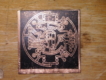
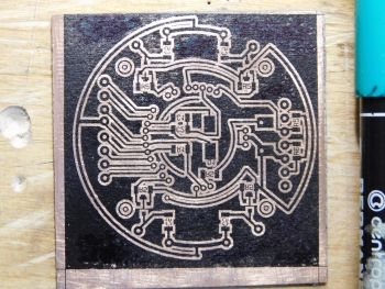
Next, we will need to wash off the non-exposed photoresist and leave only the exposed part. This can be done in 2 ways: using acetone or using caustic soda. In my case, I will wash off with caustic soda using a paint brush. Take the brush that is used to paint the pipes, that is, a small one. Soda should be diluted in 1 liter of water, only 3 grams per liter of water. Next, remove the protective word (lavsan film) and lower the board into this solution and with a brush, lightly wash off the unexposed photoresist. It happens that the lavsan film is removed quite difficult. In order to remove it quickly, the board must be put in the freezer (in the refrigerator) and kept there for 1 minute. After that, the film will be removed easily. After the photoresist is washed off, only the tracks should remain on the board, that is: the board itself was copper and of the corresponding copper color. The photoresist was blue. After washing off the photoresist in a solution of caustic soda, only blue tracks remained on the board, and the board itself became copper, that is, the color of copper. After washing off the photoresist, the board must be rinsed with tap water to wash off the solution. Rinse the board only in cold water, and when washing it is necessary to use a sponge and soap.
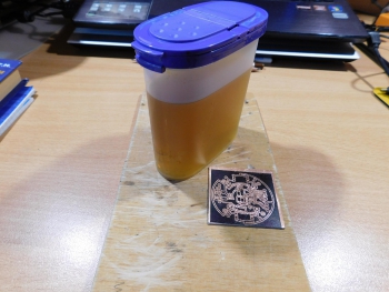
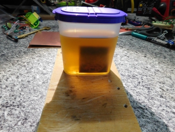
Next, the board needs to be "pickled", that is, lower it immediately into 2 solutions. You have to take it down one by one. First, we lower the board into a solution of ferric chloride, and then into monium persulfate. When working with solutions, be sure to wear rubber gloves!!!
After etching the board, they must be masked. The term mask refers to the application of a 2-component solder mask. In my case I use "RS 2000". It can be purchased at any electronics store. So, we take our board, fix it on the table in my case, I use adhesive tape and put a picture frame on it (the board), which corresponds to its size. In a word, the mask must be applied strictly in size, and any object is suitable for this, so to speak, “for equalizing”. It is worth noting that the mask is very thick, so the board must be fixed tightly. The mask itself must be applied with a rubber spatula. After applying the mask, it must be dried with a hairdryer heated to 75 degrees (no more) for 10-15 minutes. After checking manually, that is, it is trivial to touch with your hands or fingers and check whether it sticks or not. If it does not stick, then everything is fine and you need to move on to the next step.
The next step is as follows: We take our board and lay it on one glass with the tracks down, that is, the front side. Next, we take the solder mask pattern and lay it on the board, the side on which it is printed. We combine with all the tracks where there should be solder spots. After all the soldering places are combined, we clamp the pattern with the second glass. If desired, you can fasten the glass with tape so that they do not drive and do not knock down the pattern. And then, we put the board on the ultraviolet and illuminate it for 9-10 minutes. Usually 8 minutes is enough. Next, we again put the board in a solution of caustic soda and again thoroughly wash off the unexposed photoresist. But the solution already needs to be diluted with another. To wash off the solder mask, it is necessary to dilute 10 grams of caustic soda per 0.5 liter of water. It is necessary to wash off until the soldering circles (solder spots) turn white. Wash off with a paint brush.
After the solder mask is applied, the solder paths are drawn and the board is almost ready. Next, you need to apply a drawing to indicate our electronic elements or, as they say, a stencil mask (microcircuits, transistors, capacitors, etc., I hope you understand me). To do this, you need to make a silkscreen pattern pattern. And we will apply it on the front side of the board. The front side, respectively, is empty, and has not been processed in any way. It has the usual green background.
Once the stencil mask template is ready, and meets all the necessary requirements, we use the picture frame again. In my case, it is homemade and consists of cardboard. So, the board must be enclosed in a frame and matched in size with a stencil mask. After everything is combined, it is necessary to apply a little white paint to the edge of the stencil mask. Do not dilute the paint with anything, but apply, as the builders say, “paste”, that is, thick paint. Further, using a rubber construction spatula, you must first lift the template and draw a spatula over it, after applying paint to it. This is necessary in order to fill all the voids of the stencil mask. After the “run” of the paint, we directly press the template and draw it again with a spatula, evenly distributing the paint over the entire board. And the drawing is ready! It is also worth recalling that the distance between the board and the template should be 2 millimeters. You can not press the template closely. Otherwise, in the process of running the paint, the picture may turn out uneven.
Further, after the board is ready, it remains only to drill holes for soldering elements (microcircuits, capacitors, transistors, etc.). After the holes are drilled, it's time to solder all the necessary elements. But that's another story.
As you can see from the article, there is nothing complicated in the manufacture of printed circuit boards. The main knowledge and more patience.
I hope the article was of interest to everyone.
All successful board production.
Consider the process of manufacturing printed circuit boards at home using a specific example. You need to make two boards. One is an adapter from one type of housing to another. The second is the replacement of a large microcircuit with a BGA package with two smaller ones, with TO-252 packages, with three resistors. Board sizes: 10x10 and 15x15 mm. There are several options for making printed circuit boards at home. The most popular - with the help of photoresist and "iron-laser technology".
Preparing a PCB project. I use the DipTrace program: convenient, fast, high quality. Developed by our compatriots. Very convenient and pleasant user interface, in contrast to the generally recognized PCAD. Free for small projects. Libraries of cases of radio-electronic components, including 3D models. There is a conversion to PCAD PCB format. Many domestic firms have already begun to accept projects in the DipTrace format.
PCB project
The DipTrace program has the ability to see the future creation in volume, which is convenient and visual. This is what I should get (the boards are shown at different scales):
First, we mark the textolite and cut out the blank for printed circuit boards.

We output the project on a laser printer in a mirror image in the highest possible quality, without skimping on toner. Through long experiments, the best paper for this was chosen - thick matte paper for printers. You can try using photo paper or buy special thermal paper.

Clean and degrease the board blank. If there is no degreaser, you can walk on the copper foil of fiberglass with an ordinary eraser. Next, using an iron, we “weld” the toner from the paper to the future printed circuit board. I hold for 3-4 minutes under slight pressure, until the paper turns slightly yellow. I set the heat to max. I put another sheet of paper on top for more even heating, otherwise the image may “float”.
An important point here is the uniformity of heating and pressure and the heating time. If the iron is underexposed, then the print will be washed off during etching, and the tracks will be corroded by acid. If overexposed, then nearby conductors can merge with each other.

After that, put the blank with the paper stuck to it in the water. You can not wait until the textolite cools down. Photo paper gets wet quickly, and after a minute or two, you can carefully remove the top layer.

In places where there is a large accumulation of our future conductive tracks, the paper sticks to the board especially strongly. We haven't touched it yet. We give the board a couple more minutes to get wet. Now the rest of the paper is removed with an eraser or rubbing with a finger. You should get a beautiful clean blank with a clearly printed pattern.
 We remove the remnants of paper from the blank of the printed circuit board
 We take out the workpiece. We dry. If somewhere the tracks turned out to be not very clear, you can make them brighter with a thin CD marker or nail polish, for example (depending on what you are going to etch the board with).

It is necessary to ensure that all tracks come out clear, even and bright. It depends on the:
Experiment with different types of paper, different heating times, different types of fiberglass surface cleaning to find the best option in terms of quality. By choosing an acceptable combination of these conditions, in the future you will be able to produce printed circuit boards at home faster and with better quality.
We put the resulting workpiece with future conductor tracks printed on it in acid, for example, in a solution of ferric chloride. We'll talk more about other types of etching. We poison 1.5 or 2 hours. While we are waiting, we will cover the bath with a lid: the fumes are quite caustic and toxic.

We take out the finished boards from the solution, rinse, dry. Toner from a laser printer is wonderfully washed off the board with acetone. As you can see, even the thinnest conductors with a width of more than 0.2 mm came out quite well. There is very little left.

We process manufactured printed circuit boards. We wash off the remains of the flux with gasoline or an alcohol-gasoline mixture.
It remains only to cut out the boards and mount the radio elements!
With a certain skill, the “laser-ironing method” is suitable for the manufacture of simple printed circuit boards at home. Conductors from 0.2 mm and thicker are clearly obtained. The time for preparation, experiments with the selection of the type of paper and temperature of the iron, etching and tinning takes about 2 to 5 hours. When you find the optimal combination, the time spent on making the board will be less than 2 hours. This is much faster than ordering boards from a company. Cash costs are also minimal. In general, for simple budget amateur radio projects, the method is recommended for use.
Since I'm an engineering student, I often make projects at home with fairly simple electronic circuits, and for this I often make PCBs myself.
A printed circuit board (PCB) is used for mechanical mounting of radio components and their electrical connection using a conductive pattern, pads and other components etched on the copper layer of a laminated plate.
There are pre-designed copper tracks on the PCB. Properly designing connections through these traces reduces the number of wires used, and therefore the amount of damage caused by broken connections. The components are mounted on the PCB by soldering.
There are three main ways to make printed circuit boards with your own hands:
The laser etching method is industrial, so I will talk more about the first two manufacturing methods.
Typically, wiring is done by converting the circuit diagram using special programs. There are many free programs in the public domain, for example:
I created the layout using the first program.
Do not forget in the image settings (File - Export - Image) select DPIG 1200 for the best image quality.

(text on photo):
You will also need: permanent marker, sharp knife, sandpaper, paper towels, cotton wool, old clothes.
I will explain the technology using the example of manufacturing a PP touch switch with IC555.

Print the wiring diagram on a sheet of A4 glossy or photo paper on a laser printer. Do not forget:


Cut out a piece of laminate sheet the same size as the board layout image.

Scrub the foil side with a steel wool or the abrasive side of a dishwashing sponge. This is necessary to remove the oxide film and the photosensitive layer.
On a rough surface, the image fits better.


Option 1:
LUT: transfer of an image printed on a glossy layer of paper onto a foil layer of a laminate. Place the printed image on a horizontal surface with the toner facing up. Lay the board on top of the copper layer on the image. The image should be positioned exactly relative to the edges. Fasten the laminate and the image on both sides with tape so that the paper cannot move, the sticky layer of the tape should not get on the copper coating.
Option 2:
Marking the traces with a permanent marker: Using the printed wiring as a reference, mark the circuit on the copper layer of a piece of laminate, first with a pencil, then trace with a permanent black marker.


After ironing, place it in warm water for about 10 minutes. The paper will get wet and can be removed. Remove paper at a low angle and preferably without residue.
Sometimes pieces of tracks are removed with paper.
The white rectangle in the photographs marks the place where the tracks were poorly transferred and then restored with a black permanent marker.


When pickling, you need to be extremely careful.
Stir the solution lightly to make the reaction more active. The solution produces copper chloride and iron chloride.
Check every two to three minutes to see if all of the copper has been etched off the board.


Do not touch the solution with bare hands, be sure to use gloves.
The photo shows how the etching takes place.
The pickling solution is toxic to fish and other aquatic organisms.
Do not pour the used solution down the sink, it is illegal and can ruin the pipes.
Dilute the solution to reduce the concentration and only then drain into the public sewer.


The photo shows for comparison two printed circuit boards made using a LUT and a permanent marker.
put a few drops of solvent (you can use nail polish remover) on a cotton swab and remove the remaining toner from the board, you should be left with only copper tracks. Proceed with care, then dry the board with a clean cloth. Cut the board to size and sand the edges with sandpaper.
Drill mounting holes and solder all components to the board.
Printed circuit board- this is a dielectric base, on the surface and in the volume of which conductive paths are applied in accordance with the electrical circuit. The printed circuit board is designed for mechanical fastening and electrical connection between each other by soldering the leads of electronic and electrical products installed on it.
The operations of cutting a workpiece from fiberglass, drilling holes and etching a printed circuit board to obtain current-carrying tracks, regardless of the method of drawing a pattern on a printed circuit board, are performed using the same technology.
The paper on which the PCB layout is drawn is usually thin and for more accurate drilling of holes, especially when using a handmade home-made drill, so that the drill does not lead to the side, it is required to make it denser. To do this, you need to glue the printed circuit board pattern onto thicker paper or thin thick cardboard using any glue, such as PVA or Moment.

A blank of foil fiberglass of a suitable size is selected, a printed circuit board template is applied to the blank and outlined around the perimeter with a marker, a soft simple pencil, or drawing a line with a sharp object.

Next, fiberglass is cut along the marked lines using metal scissors or cut with a hacksaw. Scissors cut faster and no dust. But it must be taken into account that when cutting with scissors, fiberglass is strongly bent, which somewhat worsens the strength of gluing copper foil, and if re-soldering of the elements is required, the tracks may peel off. Therefore, if the board is large and with very thin tracks, then it is better to cut it off with a hacksaw.

A printed circuit board pattern template is glued onto the cut-out blank using Moment glue, four drops of which are applied to the corners of the blank.

Since the glue sets in just a few minutes, you can immediately start drilling holes for radio components.
It is best to drill holes using a special mini drilling machine with a 0.7-0.8 mm carbide drill. If a mini drilling machine is not available, then you can drill holes with a low-power drill with a simple drill. But when working with a universal hand drill, the number of broken drills will depend on the hardness of your hand. One drill is definitely not enough.

If the drill cannot be clamped, then its shank can be wrapped with several layers of paper or one layer of sandpaper. It is possible to wind tightly coil to coil of a thin metal wire on the shank.

After drilling is completed, it is checked whether all holes have been drilled. This is clearly visible if you look at the printed circuit board through the light. As you can see, there are no missing holes.
In order to protect the places of the foil on the fiberglass that will be conductive paths from destruction during etching, they must be covered with a mask that is resistant to dissolution in an aqueous solution. For the convenience of drawing tracks, it is better to pre-mark them with a soft, simple pencil or marker.
Before marking, it is necessary to remove traces of Moment glue, which glued the printed circuit board template. Since the glue has not hardened much, it can be easily removed by rolling it with your finger. The surface of the foil must also be degreased with a rag with any agent, such as acetone or white spirit (as refined gasoline is called), and any dishwashing detergent, such as Ferry, can also be used.

After marking the tracks of the printed circuit board, you can begin to apply their pattern. Any waterproof enamel is well suited for drawing tracks, for example, alkyd enamel of the PF series, diluted to a suitable consistency with a white spirit solvent. You can draw tracks with different tools - a glass or metal drawing pen, a medical needle and even a toothpick. In this article, I will show you how to draw PCB tracks using a drawing pen and a ballerina, which are designed to be drawn on paper with ink.

Previously, there were no computers and all the drawings were drawn with simple pencils on whatman paper and then transferred with ink to tracing paper, from which copies were made using copiers.
Drawing a picture begins with contact pads, which are drawn with a ballerina. To do this, you need to adjust the gap of the sliding jaws of the drawer of the ballerina to the required line width and to set the diameter of the circle, adjust the second screw by moving the drawer from the axis of rotation.
Next, the drawer of the ballerina for a length of 5-10 mm is filled with paint with a brush. For applying a protective layer on a printed circuit board, paint of the PF or GF brand is best suited, as it dries slowly and allows you to work calmly. NC brand paint can also be used, but it is difficult to work with it, as it dries quickly. The paint should lay down well and not spread. Before drawing, the paint must be diluted to a liquid consistency, adding a suitable solvent to it little by little with vigorous stirring and trying to draw on scraps of fiberglass. To work with paint, it is most convenient to pour it into a nail polish bottle, in the twist of which a solvent-resistant brush is installed.
After adjusting the drawer of the ballerina and obtaining the required line parameters, you can begin to apply contact pads. To do this, the sharp part of the axis is inserted into the hole and the base of the ballerina is rotated in a circle.

With the correct setting of the drawing pen and the desired consistency of paint around the holes on the printed circuit board, circles of perfectly round shape are obtained. When the ballerina begins to draw poorly, the remnants of dried paint are removed from the drawer gap with a cloth and the drawer is filled with fresh paint. to outline all the holes on this printed circuit board with circles, it took only two refills of the drawing pen and no more than two minutes of time.
When the round contact pads on the board are drawn, you can start drawing conductive tracks using a manual drawing pen. The preparation and adjustment of a manual drawing pen is no different from the preparation of a ballerina.
The only thing that is additionally needed is a flat ruler, with pieces of rubber glued on one of its sides along the edges, 2.5-3 mm thick, so that the ruler does not slip during operation and the fiberglass, without touching the ruler, can freely pass under it. A wooden triangle is best suited as a ruler, it is stable and at the same time can serve as a support for the hand when drawing a printed circuit board.

So that the printed circuit board does not slip when drawing tracks, it is advisable to place it on a sheet of sandpaper, which is two sandpaper sheets riveted together with paper sides.

If, when drawing paths and circles, they touched, then no action should be taken. It is necessary to allow the paint on the printed circuit board to dry to a state where it will not stain when touched, and use the edge of a knife to remove the excess part of the pattern. In order for the paint to dry faster, the board must be placed in a warm place, for example, in winter, on a radiator. In the summer season - under the rays of the sun.

When the pattern on the printed circuit board is completely applied and all defects are corrected, you can proceed to etching it.
When printing on a laser printer, the image formed by the toner is transferred electrostatically from the photo drum, on which the laser beam painted the image, onto paper. The toner is held onto the paper, preserving the image, only due to electrostatics. To fix the toner, the paper is rolled between rollers, one of which is a thermal oven heated to a temperature of 180-220°C. The toner melts and penetrates the texture of the paper. After cooling, the toner hardens and adheres firmly to the paper. If the paper is heated again to 180-220°C, the toner will again become liquid. This property of the toner is used to transfer the image of current-carrying tracks to a printed circuit board at home.
After the file with the printed circuit board drawing is ready, it is necessary to print it using a laser printer on paper. Please note that the image of the printed circuit board drawing for this technology must be viewed from the side of the installation of parts! An inkjet printer is not suitable for these purposes, as it works on a different principle.
If you print a printed circuit board pattern on ordinary paper for office equipment, then due to its porous structure, the toner will penetrate deeply into the body of the paper and when the toner is transferred to the printed circuit board, most of it will remain in the paper. In addition, there will be difficulties with removing paper from the printed circuit board. You will have to soak it in water for a long time. Therefore, to prepare a photomask, you need paper that does not have a porous structure, such as photographic paper, a substrate from self-adhesive films and labels, tracing paper, pages from glossy magazines.
As the paper for printing the PCB design, I use tracing paper from old stock. Tracing paper is very thin and it is impossible to print a template directly on it, it jams in the printer. To solve this problem, before printing on a piece of tracing paper of the required size, apply a drop of any glue in the corners and stick it on a sheet of A4 office paper.

This technique allows you to print a printed circuit board pattern even on the thinnest paper or film. In order for the toner thickness of the pattern to be maximum, before printing, you need to configure the “Printer Properties” by turning off the economical printing mode, and if this function is not available, then select the roughest type of paper, such as cardboard or something like that. It is quite possible that you will not get a good print the first time, and you will have to experiment a little, choosing the best print mode for a laser printer. In the resulting print of the pattern, the tracks and contact pads of the printed circuit board must be dense without gaps and smearing, since retouching is useless at this technological stage.

It remains to cut the tracing paper along the contour and the template for the manufacture of the printed circuit board will be ready and you can proceed to the next step, transferring the image to the fiberglass.
Transferring the PCB pattern is the most critical step. The essence of the technology is simple, paper, with the side of the printed pattern of the tracks of the printed circuit board, is applied to the copper foil of the fiberglass and pressed with great effort. Next, this sandwich is heated to a temperature of 180-220°C and then cooled to room temperature. The paper is torn off, and the pattern remains on the printed circuit board.
Some craftsmen suggest transferring a pattern from paper to a printed circuit board using an electric iron. I tried this method, but the result was unstable. It is difficult to simultaneously heat the toner to the desired temperature and evenly press the paper against the entire surface of the printed circuit board when the toner solidifies. As a result, the pattern is not completely transferred and there are gaps in the pattern of PCB tracks. It is possible that the iron did not heat up enough, although the regulator was set to the maximum heating of the iron. I did not want to open the iron and reconfigure the thermostat. Therefore, I used another technology that is less laborious and provides a 100% result.
On a printed circuit board cut to size and degreased with acetone, a blank of foil fiberglass was glued to the corners of a tracing paper with a pattern printed on it. On top of the tracing paper put, for a more uniform pressure, heels of sheets of office paper. The resulting package was placed on a sheet of plywood and covered with a sheet of the same size on top. This whole sandwich was clamped with maximum force in the clamps.

It remains to heat the made sandwich to a temperature of 200 ° C and cool. An electric oven with a temperature controller is ideal for heating. It is enough to place the created structure in a cabinet, wait for the set temperature to reach, and after half an hour remove the board for cooling.

If an electric oven is not available, then you can also use a gas oven by adjusting the temperature with the gas supply knob according to the built-in thermometer. If there is no thermometer or it is faulty, then women can help, the position of the regulator knob, at which pies are baked, will do.

Since the ends of the plywood were warped, just in case, I clamped them with additional clamps. to avoid this phenomenon, it is better to clamp the printed circuit board between metal sheets 5-6 mm thick. You can drill holes in their corners and clamp the printed circuit boards, tighten the plates with screws and nuts. M10 will be enough.
After half an hour, the design has cooled down enough for the toner to harden, the board can be removed. At the first glance at the removed printed circuit board, it becomes clear that the toner transferred from the tracing paper to the board perfectly. The tracing paper fit snugly and evenly along the lines of the printed tracks, the rings of the pads and the marking letters.

The tracing paper easily came off almost all tracks of the printed circuit board, the remains of the tracing paper were removed with a damp cloth. But still, there were gaps in several places on the printed tracks. This can happen as a result of uneven printing of the printer or remaining dirt or corrosion on the fiberglass foil. Gaps can be filled with any waterproof paint, nail polish or retouched with a marker.

To check the suitability of a marker for retouching a printed circuit board, you need to draw lines on paper with it and moisten the paper with water. If the lines do not blur, then the retouching marker is suitable.

Etching a printed circuit board at home is best in a solution of ferric chloride or hydrogen peroxide with citric acid. After etching, the toner from the printed tracks is easily removed with a swab dipped in acetone.
Then holes are drilled, conductive paths and contact pads are tinned, and radioelements are soldered.

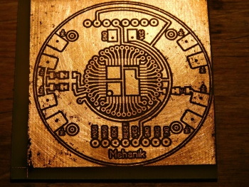
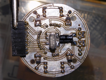
This form was taken by a printed circuit board with radio components installed on it. The result was a power supply and switching unit for an electronic system that complements an ordinary toilet bowl with a bidet function.
To remove copper foil from unprotected areas of foil fiberglass in the manufacture of printed circuit boards at home, radio amateurs usually use a chemical method. The printed circuit board is placed in an etching solution and, due to a chemical reaction, the copper, unprotected by the mask, dissolves.
Depending on the availability of components, radio amateurs use one of the solutions shown in the table below. Etching solutions are listed in order of popularity for their use by radio amateurs in the home.
| Solution name | Compound | Quantity | Cooking technology | Advantages | Flaws |
|---|---|---|---|---|---|
| Hydrogen peroxide plus citric acid | Hydrogen peroxide (H 2 O 2) | 100 ml | Dissolve citric acid and table salt in a 3% hydrogen peroxide solution | Availability of components, high pickling rate, safety | Not stored |
| Citric acid (C 6 H 8 O 7) | 30 g | ||||
| Salt (NaCl) | 5 g | ||||
| Aqueous solution of ferric chloride | Water (H2O) | 300 ml | Dissolve ferric chloride in warm water | Sufficient etching rate, reusable | Low availability of ferric chloride |
| Ferric chloride (FeCl 3) | 100 g | Hydrogen peroxide plus hydrochloric acid | Hydrogen peroxide (H 2 O 2) | 200 ml | Pour 10% hydrochloric acid into a 3% hydrogen peroxide solution | High pickling rate, reusable | Requires high precision |
| Hydrochloric acid (HCl) | 200 ml | ||||
| Aqueous solution of copper sulphate | Water (H2O) | 500 ml | In hot water (50-80 ° C), dissolve table salt, and then blue vitriol | Component Availability | The toxicity of copper sulfate and slow etching, up to 4 hours |
| Copper sulfate (CuSO 4) | 50 g | ||||
| Salt (NaCl) | 100 g | ||||
Etch printed circuit boards in metal utensils are not allowed. To do this, use a container made of glass, ceramic or plastic. It is allowed to dispose of the spent pickling solution into the sewer.
A solution based on hydrogen peroxide with citric acid dissolved in it is the safest, most affordable and fastest working. Of all the listed solutions, by all criteria, this is the best.

Hydrogen peroxide can be purchased at any pharmacy. Sold in the form of a liquid 3% solution or tablets called hydroperite. To obtain a liquid 3% solution of hydrogen peroxide from hydroperite, you need to dissolve 6 tablets weighing 1.5 grams in 100 ml of water.
Citric acid in the form of crystals is sold in any grocery store, packaged in bags weighing 30 or 50 grams. Table salt can be found in any home. 100 ml of pickling solution is enough to remove 35 µm thick copper foil from a 100 cm2 printed circuit board. The spent solution is not stored and cannot be reused. By the way, citric acid can be replaced with acetic acid, but because of its pungent smell, you will have to pickle the printed circuit board in the open air.
The second most popular pickling solution is an aqueous solution of ferric chloride. Previously, it was the most popular, since ferric chloride was easy to get at any industrial enterprise.

The etching solution is not picky about the temperature, it etchs rather quickly, but the etching rate decreases as the ferric chloride in the solution is consumed.

Ferric chloride is very hygroscopic and therefore quickly absorbs water from the air. As a result, a yellow liquid appears at the bottom of the jar. This does not affect the quality of the component and such ferric chloride is suitable for the preparation of an etching solution.
If the used solution of ferric chloride is stored in an airtight container, then it can be used repeatedly. To be regenerated, it is enough to pour iron nails into the solution (they will immediately be covered with a loose layer of copper). Leaves hard-to-remove yellow spots upon contact with any surface. At present, a solution of ferric chloride for the manufacture of printed circuit boards is used less frequently due to its high cost.
Excellent pickling solution, provides high pickling speed. Hydrochloric acid, with vigorous stirring, is poured into a 3% aqueous solution of hydrogen peroxide in a thin stream. Pouring hydrogen peroxide into acid is unacceptable! But due to the presence of hydrochloric acid in the etching solution, great care must be taken when etching the board, since the solution corrodes the skin of the hands and spoils everything it gets on. For this reason, an etching solution with hydrochloric acid at home is not recommended.
The method of manufacturing printed circuit boards using copper sulphate is usually used if it is impossible to manufacture an etching solution based on other components due to their unavailability. Copper sulfate is a pesticide and is widely used for pest control in agriculture. In addition, the PCB etching time is up to 4 hours, while it is necessary to maintain the temperature of the solution at 50-80°C and ensure that the solution is constantly changed at the etched surface.
For etching the board in any of the above etching solutions, glass, ceramic or plastic utensils, such as dairy products, are suitable. If there was no suitable container size at hand, then you can take any box made of thick paper or cardboard of a suitable size and line its inside with plastic wrap. An etching solution is poured into the container and a printed circuit board is carefully placed on its surface with a pattern down. Due to the forces of the surface tension of the liquid and the low weight, the board will float.

For convenience, a cork from a plastic bottle can be glued to the center of the board with glue. The cork will simultaneously serve as a handle and a float. But there is a danger that air bubbles form on the board and in these places the copper will not corrode.

To ensure uniform etching of copper, you can put the printed circuit board on the bottom of the tank with the pattern up and periodically shake the bath with your hand. After a while, depending on the pickling solution, areas without copper will begin to appear, and then the copper will completely dissolve on the entire surface of the printed circuit board.

After the final dissolution of copper in the pickling solution, the printed circuit board is removed from the bath and thoroughly washed under running water. The toner is removed from the tracks with a rag soaked in acetone, and the paint is well removed with a rag soaked in a solvent that was added to the paint to obtain its desired consistency.
The next step is to prepare the printed circuit board for the installation of radio elements. After removing the paint from the board, the tracks must be processed in a circular motion with fine sandpaper. You don’t need to get carried away, because the copper tracks are thin and can be easily grinded off. Just a few passes with a low-pressure abrasive is sufficient.

Further, the current-carrying tracks and contact pads of the printed circuit board are covered with an alcohol-rosin flux and tinned with soft solder with an electric soldering iron. so that the holes on the printed circuit board are not tightened with solder, you need to take a little of it on the soldering iron tip.

After completing the manufacture of the printed circuit board, all that remains is to insert the radio components into the intended positions and solder their leads to the sites. Before soldering, the legs of the parts must be moistened with alcohol-rosin flux. If the legs of the radio components are long, then they must be cut with side cutters before soldering to a protrusion length of 1-1.5 mm above the surface of the printed circuit board. After completing the installation of the parts, it is necessary to remove the remains of rosin using any solvent - alcohol, white spirit or acetone. They all successfully dissolve rosin.

This simple capacitive relay circuit took no more than five hours to complete from the PCB traces to a working prototype, much less than the layout of this page.
PCB manufacturing technology at home
"... and experience is the son of difficult mistakes ..."
So, the board manufacturing process begins with a schematic diagram of the future device. At this stage, you determine not only how the components will be connected to each other, but also decide which components are suitable for your design. For example: use standard parts or SMD (which, by the way, also come in various sizes). The size of the future fee will depend on this.
Next, we decide on the choice of software with which you will draw the future board. If a circuit diagram can be drawn by hand, then with a printed circuit board drawing it will not work out that way (especially when it comes to SMD components). I use . I downloaded it a long time ago and I use it. A very good program, with an intuitive interface, nothing more. In the program we create a drawing of a printed circuit board.
Haven't revealed any secrets yet? So: when the board drawing has already been created, you have made sure that the location of the components is correct, you should set the "ground" i.e. fill the gaps between the tracks and holes, for this the program has a special function that does this automatically (the default is a gap of 0.4 mm). Why is this needed? To make etching (we will discuss it later) in less time, it will be easier for you to control the process and it is also useful to do this from circuit design considerations ...

Note: When designing the board, try not to make holes smaller than 0.5mm in diameter, unless of course you have a special machine for drilling holes, but more on that later...
Excellent! We have drawn a drawing of the future printed circuit board, now it needs to be printed on a LASER printer (Lut means laser). To do this, click the print. The above program creates a special file, while you can choose the number of copies, their location, make a frame, specify the size of the holes and mirror.
Note: if you are making a double-sided printed circuit board, then the front part must be reflected horizontally, and the wrong side should be left as is. ConcerningSprint- layout, then it is better to do this at the stage of creating the circuit, and not at the stage of preparing the file for printing, since there are "glitches" with the "mass", it disappears, in places.
And yet, it is better to print several copies, even if you only need one copy, because defects may appear in the next steps and in order not to run to the printer every time, do it in advance.
What to print on? To begin with, we print on a regular sheet of paper to make sure for the last time that everything is done correctly, that all components are the right size. This will also warm up the printer.

Now we set the maximum density of the toner, disable all saving modes (by the way, it is better to use a fresh cartridge). We take a substrate from self-adhesive paper, better from "velvet" (it gives the best result, maybe this is due to the fact that it is thicker), insert the shiny side into the printer and click on "print". Ready!

Note: from now on, you can not touch this paper, only by the edges, otherwise you can smudge the drawing!
About the reuse of the substrate. Let's say that you printed a drawing, and it took up only half of the sheet, you don't need to throw away the other half, you can also print on it, BUT! for some reason, when reprinting, the printer "chews" paper in 20% of cases, so be careful!
We prepare textolite
I use a regular foil fiberglass 1 mm thick, which is sold in a radio parts store. Since we want to make a double-sided board, we buy a double-sided textolite. We cut off the desired piece, no need to make a stock, it will not be needed. Cut off. We take a zero skin and skin the textolite to a shine on both sides, if small scratches remain, then it's okay, the toner will hold on better (but without fanaticism!). Next, we take acetone (alcohol) and wipe the board on both sides to degrease it. Ready!

Note: when you are sanding the textolite, pay attention to the corners of the board, very often they are “under-sanded” or, even worse, “re-sanded”, this is when there is no foil left at all. After wiping with acetone, the board also cannot be touched by hands, you can only take it by the edges, preferably with tweezers.


Next is the most crucial stage: transferring the pattern from paper to textolite. It is done with the help of an iron (lut means iron). Anyone will do here. We heat it up to 200 degrees (often this is the maximum temperature of the iron, so we just bring the regulator to the maximum and wait for it to heat up).
Now here are the secrets! To transfer the printed circuit board pattern from paper to textolite, it is necessary to attach the paper to the textolite with the right side, then press down with an iron and smooth it well. Like nothing complicated? But the most difficult thing is to apply the iron so as not to sweep the paper, especially if the handkerchief is small and you make it in a single copy, besides, it is not so easy to use the iron. There is an interesting way to make the task easier.
Note: We are looking at making double-sided printed circuit boards, so a little about paper preparation. In some sources, it is advised to do this: we transfer one side, seal the opposite with adhesive tape or electrical tape, poison one side, then drill holes, combine the pattern of the other side, then transfer it again, glue it, poison it. This takes a lot of time, because, in fact, you need to pickle two boards! You can speed up the process.
We take two pieces of paper, on which there is a drawing from the front and back sides, we combine them. This is best done on a window pane or on a transparent backlit table. Note! in this case, it is necessary to cut off the papers with a margin, the more the better, but without fanaticism, 1-1.5 cm is enough. We fasten them with a stapler from 3 sides (no glue!), We get an envelope in which we put the board and align it.

The most interesting. We take two pieces of textolite (see the size in the figure), put them with the foil side to each other, and place an “envelope” with the board between them, and fix the edges of this sandwich with paper clips so that the textolite sheets do not move relative to each other.

Note: for these purposes, it is better to choose a thinner textolite, it will warm up faster, and will be able to deform where necessary.
Now, we take the iron and calmly apply it to our sandwich, and we press with all our strength, first on one side, then turn it over and press on the other. For the best effect, after the first pressure, I recommend making several circular movements with the iron to be sure that the paper is pressed in all places. You don’t need to iron for a long time, usually no more than 1-3 minutes for everything, but no one will tell you the exact time, because it depends on the size of the board, the amount of toner. The main thing is not to overexpose, because in this case the toner can simply spread, and if it is underexposed, the drawing may not be completely transferred. Practice, folks, practice!
Then you can open the sandwich and make sure that the paper is stuck to the textolite on all sides, i.e. no air bubbles. And we quickly carry a fee under running water, and cool it (with cold water, of course).
Note: If you used a substrate from self-adhesive paper, then under water it falls off by itself from the textolite and the board quietly falls out of the envelope. If you used a velvet paper backing (thicker), then this will not work with it. We take scissors and cut off the sides of the envelope, then read slowly, holding the edge of the paper, under running water, remove the paper. As a result, no toner should remain on the paper, it will all be on the textolite.
At this stage, if defects occur, there are two ways to proceed. If there are too many defects, it is better to take acetone, wash off the toner from the textolite and try again (after repeating the process of cleaning the textolite with sandpaper).
An example of an irreparable defect (in this case, I started over):


If there are few defects, then you can take a marker for drawing printed circuit boards and supplement the flaws.
A good option, there are small holes in the "mass", but they can be painted over with a marker:

Corrected options. The green shaded areas are clearly visible:

Great, this was the most technologically difficult stage, then it will be easier.
Now you can pickle the board, i.e. remove excess foil from the textolite. The essence of etching is as follows: we place the board in a solution that corrodes the metal, while the metal under the toner (under the board pattern) remains unharmed, and the one around is removed.
I will say a few words about the solution. To poison, in my opinion, is better with ferric chloride, it is not expensive, it is very simple to prepare the solution, and in general it gives a good result. The recipe is simple: 1 part ferric chloride, 3 parts water and that's it! But there are other methods of etching.
Note: it is necessary to add water to the iron, and not vice versa, so it is necessary!
Note: There are two types of ferric chloride (which I have seen): anhydrous and 6-aqueous. Anhydrous, as the name implies, completely dry, and in the container in which it is sold there is always a lot of dust, this is not a problem. But when water is added, they will actively dissolve, there is a strong exothermic reaction (the solution heats up), with the release of some kind of gas (most likely it is chlorine or hydrogen chloride, well, everything is the same - a rare dirty trick), which CANNOT be inhaled, I recommend diluting it in air.
But 6-water iron is already better. This, in fact, is already a solution, water is added, wet lumps are obtained, which also need to be added to the water, but there is no such violent reaction anymore, the solution heats up, but not very quickly and not very strongly, but everything is safe and quiet (windows are still needed open).

Note: the advice that I give here is not the only correct one, on many forums you can meet people who get boards at a different concentration, a different grade of ferric chloride, etc. I just tried to summarize the most popular tips and personal experience. So, if these methods did not help, then try another method and you will succeed!
Have you prepared a solution? Excellent! Choose a capacity. For one-sided, this choice is simple, we take a transparent (to see the etching process) plastic box with a lid, put the board on the bottom. But with double-sided boards, things are not so simple. It is necessary that the etching speed on each side be approximately the same, otherwise a situation may arise when one side has not yet been etched, and the tracks are already dissolving on the other. To prevent this from happening, you need to place the board vertically in the tank (so that it does not lie on the bottom), then the solution around will be homogeneous and the etching rate will be approximately the same. Therefore, it is necessary to take a high capacity in order for the board to fit in the "full height". It is better to choose a narrow transparent jar so that you can observe the etching process.
Next, the solution must be heated (put on a battery), this will increase the rate of the reaction, and shake it periodically to ensure uniform etching and to avoid the appearance of sediment on the board.
Note: someone puts it in the microwave and heats it there, but I don’t recommend you do this, because. I read on one forum that after this you can get poisoned by food from this microwave. There is no direct evidence, but it is better not to risk it!
Note: to ensure the uniformity of etching, you need to mix the solution (shake the container), but there are more technologically advanced methods. You can attach a bubble generator (from the aquarium) to the tank and then the bubbles will mix the solution. I've seen people make servo oscillating etching pots with a microcontroller that "shakes" according to a special algorithm! Here I do not consider in detail each option, because each has its own nuances and the article would then be very long. I described the easiest way, which is perfect for the first boards.
Wait, no need to rush!
To understand that the etching process has ended is very simple: there will be no trace of foil between the black toner. When this happens, you can withdraw the fee.
Then we carry it under water and wash off the remnants of the solution. We take alcohol or acetone and wash off the toner, foil tracks should remain under it. Great, is everything okay? Anywhere there are no "poisonous" places? Anywhere there are no "over-etched" places? Great! We can move on!

Note: When defects appear, this stage of production presents you with a serious choice: discard the defect and start over, or try to fix it. It depends on how serious the defects are and how high the demands you place on your work.
The next step is tinning the board. There are two main ways. The first one is the simplest. We take a flux for soldering (I use LTI-120, but not the one that looks like rosin varnish, which leaves terrible spots on the soldering field, but on an alcohol basis, it is much lighter), we generously lubricate the board with it on one side. We take solder and a soldering iron with a wide tip and begin to tin the board, i.e. cover the entire foil with solder.

Note: do not keep the soldering iron on the tracks for too long, because. textolite is of different quality and some tracks fall off very easily, especially thin ones. Be careful!
In this case, solder “streaks” or unpleasant-looking tubercles may appear on the board, it is better to deal with them with the help of a desoldering braid. In those places where it is necessary to remove excess solder, we conduct it, all excess solder is removed and a flat surface remains.
Note: you can immediately wrap the braid around the sting and tin it right away, it might even be easier.


The method is good, but in order to achieve an aesthetic appearance of the board, some experience and skill are required.
The second way is more difficult. You will need a metal container in which you can boil water. Pour water into a container, add a couple of tablespoons of citric acid and put on gas, bring to a boil. Solder should be chosen not simple, but with a low melting point, for example, Rose alloy (about 100 degrees Celsius). We throw a few balls to the bottom and see that they have melted. Now we throw the board on these balls, then we take a stick (preferably a wooden one, so as not to burn our hands), wrap it with cotton and start rubbing the board, disperse the solder along the tracks, so you can achieve an even distribution of solder over the entire board.
The method is quite good, but more expensive, and you need to pick up a container, because you have to wield tools in it. It is better to use something with low sides.
Note: you will have to do this operation for quite some time, so it is better to open the window. With experience, you should get faster.
Note: many people do not speak well of Rosé's alloy due to its brittleness, but for tinning boards in this way, it is very suitable.
Note: I myself do not like this method, because I tried to use it when I made the first board and I remember well how inconvenient it was to "cook" this board in a tin can without tools .... Oh, it was terrible! But now...
Both methods have their advantages and disadvantages, the choice depends only on you and your capabilities, desires, skills.
Note: Next, I recommend ringing the board with a multimeter to make sure that there are no intersections of tracks anywhere that should not intersect, that there are no random "snots" anywhere, or some other surprise. If a problem is found, we take a soldering iron and remove excess solder, if it does not help, then we use a clerical knife and carefully separate the necessary places. This may mean that the board is not etched in some places, but that's okay.
To do this, use a small drill and a drill. Now special drills for printed circuit boards are sold with special sharpening and special grooves on the drill. At first I used a regular drill for metal with a thickness of 0.6 mm, then I switched to a special one and the result is very good. Firstly, even with my budget drill, any textolite is drilled without any problems, with almost no effort. The drill itself "bites" into it and pulls the tool along with it. Secondly, it leaves a neat inlet and outlet, without burrs, in contrast to a standard drill, which literally "tears" the textolite. Thirdly, this drill almost does not slip, i.e. you just need to get to the right place the first time and it will not go anywhere. Miracle, not a tool! But it also costs a little more than a regular drill.
Note: In order to "get into the right place right away" it is better to use an awl or a special tool for punching, just do not make too deep notches, this can point the drill in the wrong direction. Another thing: this drill has one drawback - it breaks easily, so it's better to use a special machine to drill holes or hold the drill strictly vertically. Believe me, it breaks very easily! Especially when you need to drill a hole of 0.3 mm or 0.2 mm, but this is already jewelry work.
Ready! That's actually all! We solder the through holes with thin wires and we get neat hemispheres on the board, it looks very personal. Now all you have to do is solder all the components of the circuit and make sure it works, but that's a topic for another article. And here's what happened to me:

That's all. Once again I want to emphasize that here I only tried to summarize all the materials that I managed to find about LUT, and my experience. It turned out a bit long, but in every case there are many nuances that must be taken into account in order to achieve the best result. The last piece of advice I can give you is to try, try to make boards, because skill comes with experience. And in the end I will give an epigraph once again: "... and experience is the son of difficult ERRORS ..."
If you have any questions, you can leave them in the comments. I would also appreciate constructive criticism.
If you adhere to proper nutrition, then avocados are probably in ...


Pizza can be cooked not only with meat products - sausage, sausages and ...